In the first and in-between posts I leaned on “symbols left in the firmware” a few times without saying how I got hold of that firmware. This post covers that. There are gentle ways to pull firmware off a device, and there is the sledgehammer: pry the case open, lift the flash chip off the board with hot air, and read it in a socket. My controller was dead anyway, so the sledgehammer it is.
What’s on the board
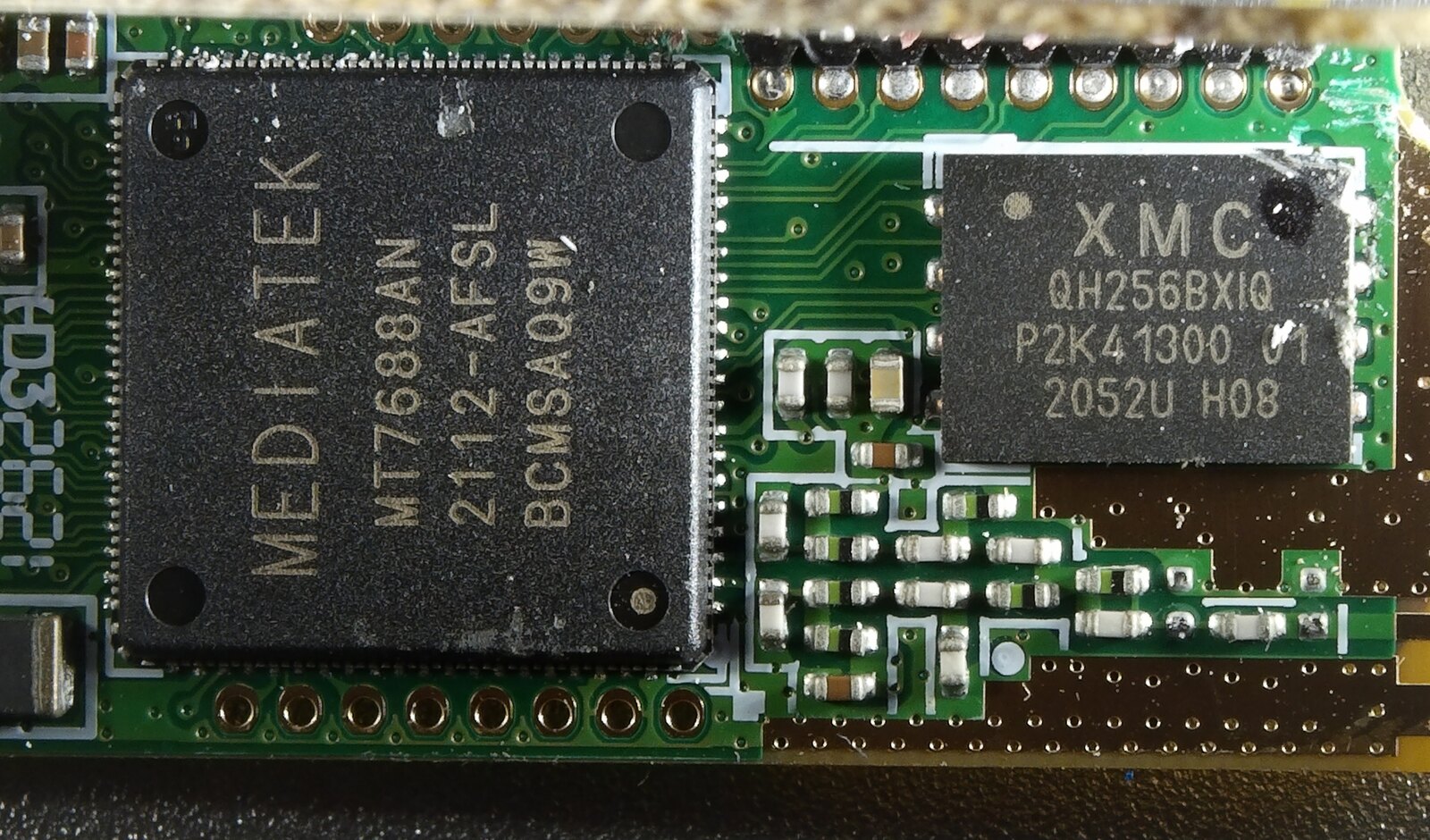
The controller is a small board built around a MediaTek MT7688AN, a MIPS SoC that usually turns up in cheap WiFi routers and IoT widgets. Next to it sits the part I care about: an XMC XM25QH256B, a 256 Mbit (32 MiB) 3.3V SPI NOR flash in an 8-pad WSON package. That chip holds the bootloader, the Linux kernel, the root filesystem and the device’s own user data. Get a copy of it and you have everything the controller runs.
One quirk worth noting: flashrom reads the XM25QH256B fine if you tell it the chip is an XM25QH256C. The B revision is not in its database, but the C one behaves the same for a read.
Opening the case
There are no screws. The case is ultrasonically welded plastic, so it is designed to be opened exactly once. I pried it apart along the seam, and in the process the PCB sandwich inside came apart with it. By the time I was in, the case and the board stack were both firmly in the non-repairable category. That was fine here, since the controller was already dead and I was after the flash chip, not a working unit. If you want to keep yours alive, this is not the method.
Getting the chip off
You can try to read an SPI flash in-circuit, with a clip on the chip while it is still soldered down. Sometimes that works. Often it does not, because the rest of the board is powered through the same pins and fights you for control of the bus, or the SoC starts booting the moment you apply power.
The sledgehammer approach is to take the chip off the board. A hot-air rework station at around 350°C, a little flux, and the WSON package lifts off its pads once the solder melts. After that it is tweezers and patience, and keeping the hot air off the neighbouring parts.
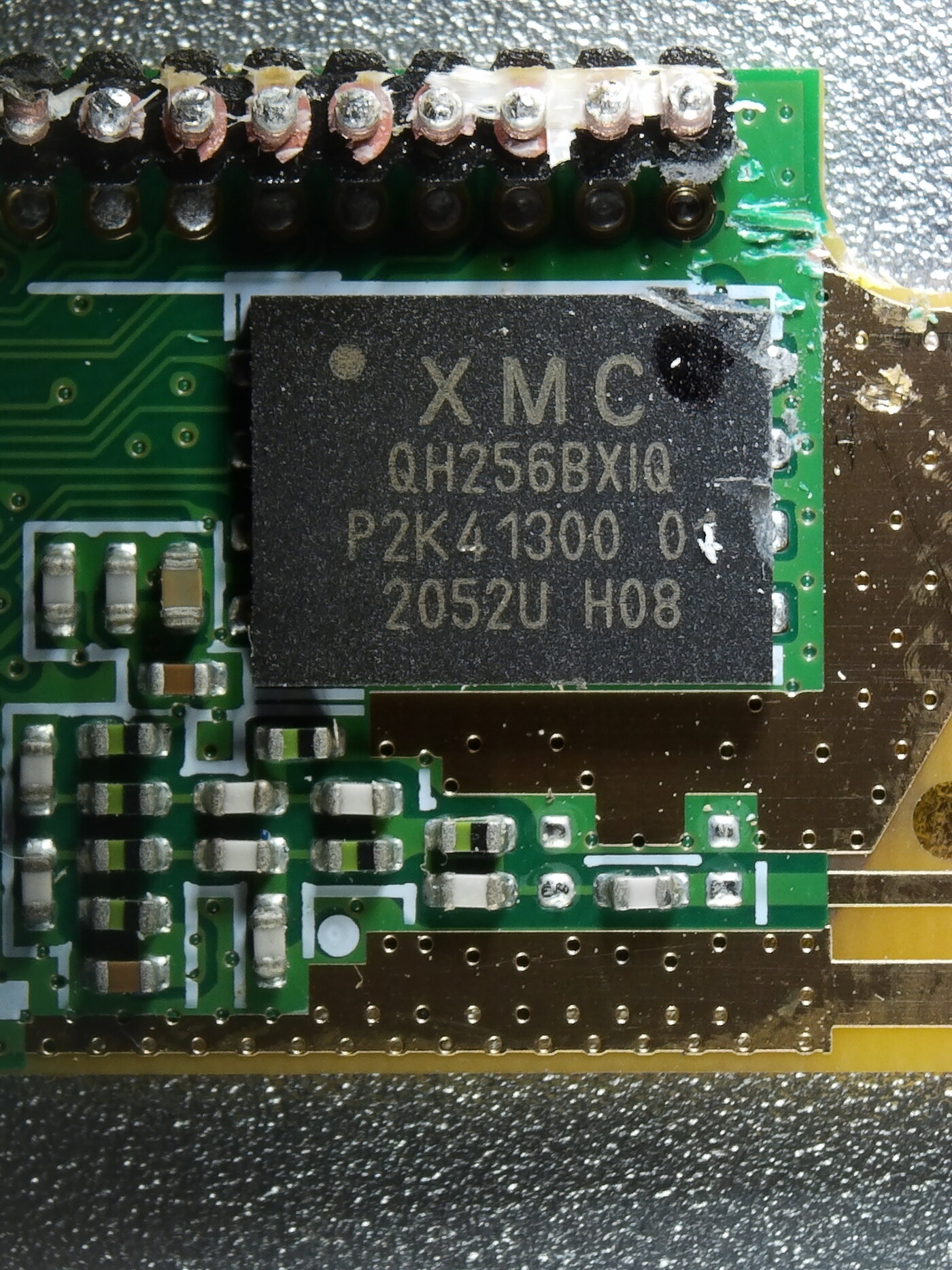
The target: the XMC QH256BXIQ (XM25QH256B) SPI NOR flash, still on the board.
With the chip free, it goes onto a WSON-to-DIP adapter, soldered down so it can stand on header pins like a DIP chip.
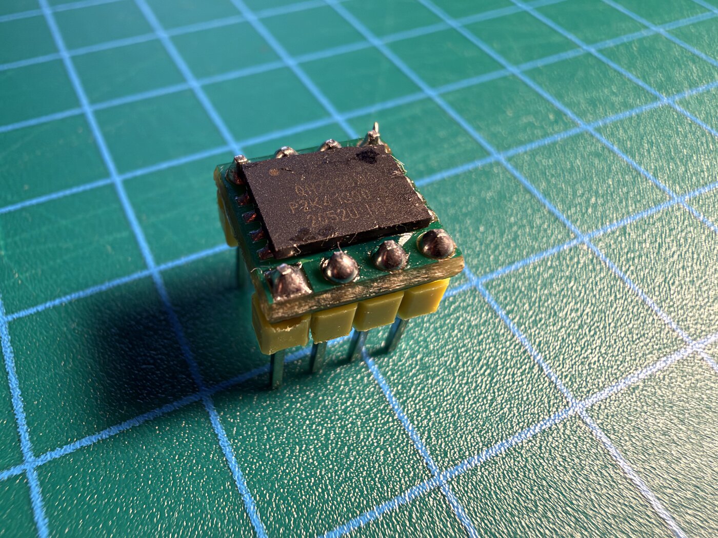
The flash on a DIP-8 adapter board, ready to drop into a socket.
From there it goes into a cheap SPI programmer. A CH341A-style reader is enough for a one-off.
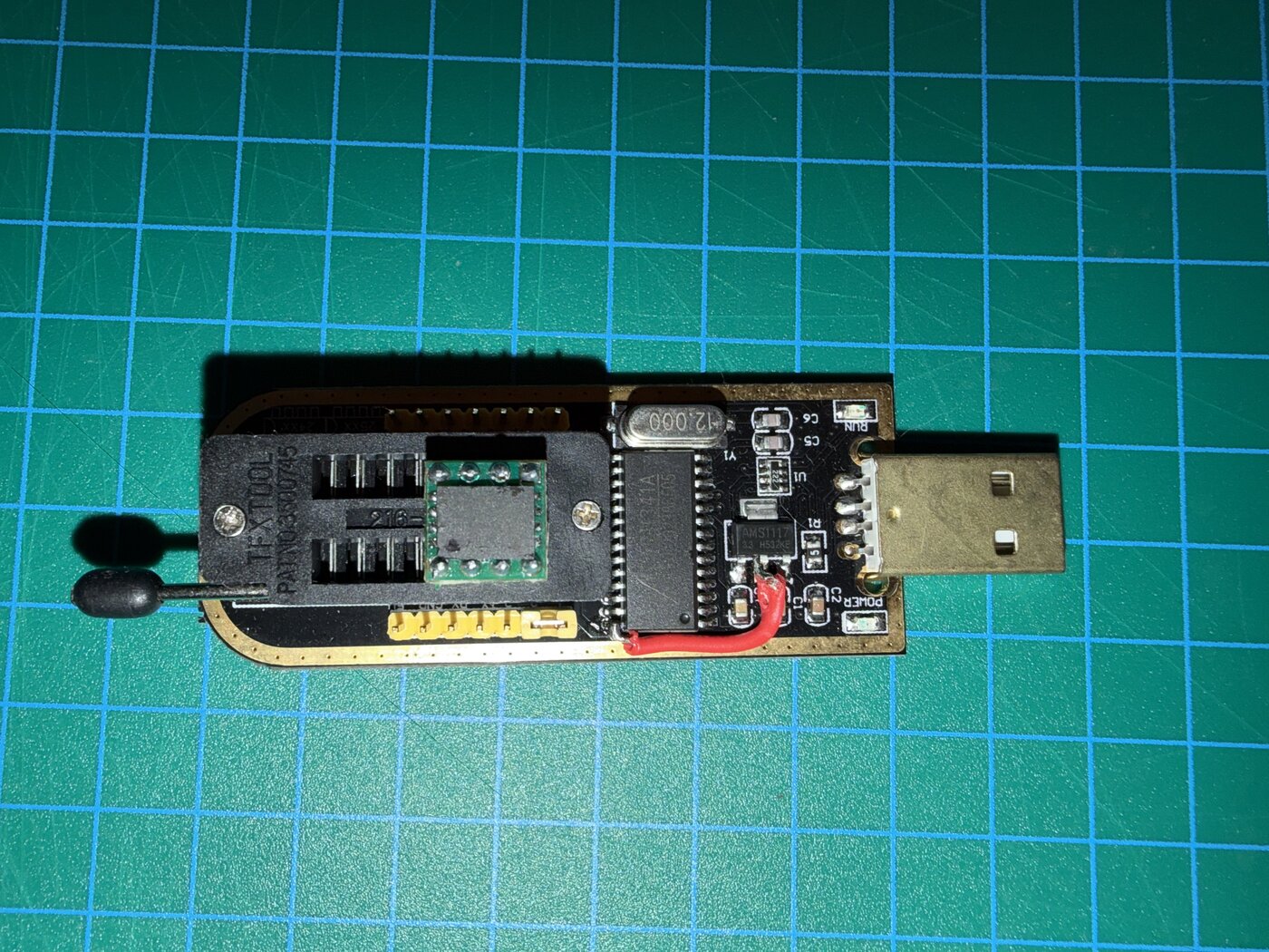
A CH341A USB programmer, a few euros online. The adapter drops straight into the socket.
flashrom does the rest:
flashrom -p ch341a_spi -c XM25QH256C -r flash.bin
A couple of minutes later you have flash.bin, a full 33,554,432-byte image of everything the controller knows.
What’s inside
The first look at any unknown image is binwalk, which scans for the signatures of known formats:
$ binwalk flash.bin

DECIMAL       HEXADECIMAL   DESCRIPTION
--------------------------------------------------------------------------------
80912         0x13C10       U-Boot version string, "U-Boot 1.1.3 (Dec 23 2020)"
327680        0x50000       uImage header, created: 2018-01-26, image size: 1351431
                            bytes, OS: Linux, CPU: MIPS, type: OS Kernel Image,
                            compression: lzma, name: "MIPS OpenWrt Linux-4.9.77"
327744        0x50040       LZMA compressed data, uncompressed size: 4305428 bytes
1679175       0x199F47      Squashfs filesystem, little endian, version 4.0,
                            compression:xz, size: 5745164 bytes, 986 inodes
29425664      0x1C10000     JFFS2 filesystem, little endian
That is the whole flash in five lines. Laid out across the 32 MiB:
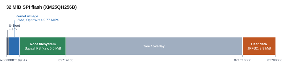
The flash layout, as found by binwalk. A standard OpenWrt-style arrangement: bootloader, kernel, read-only root, and a writable user-data partition at the top.
- U-Boot 1.1.3 as the bootloader, at the very start of the flash.
- A uImage kernel: Linux 4.9.77, MIPS, LZMA-compressed, built as part of OpenWrt.
- A SquashFS root filesystem, xz-compressed. This is the read-only system image.
- A large stretch of free space and overlay.
- A JFFS2 partition at the top of the flash. This is the writable area, holding WiFi credentials, the panel layout, animations and the like.
Under the badge, it is an ordinary OpenWrt device.
Dumping the filesystems
binwalk can carve and extract on its own, but I did it by hand to know exactly what I had. Cut out each partition with dd using the offsets above, then unpack it with the right tool.
The SquashFS root comes out with unsquashfs:
dd if=flash.bin of=squashfs bs=1 skip=$((0x199F47))
unsquashfs -d squashfs-root squashfs
The JFFS2 partition needs a JFFS2 reader. jefferson handles it:
dd if=flash.bin of=jffs2 bs=1 skip=$((0x1C10000))
jefferson jffs2 -d jffs2-root
With that, the whole controller is sitting in two directories on my laptop.
First look around
The root filesystem is OpenWrt. It is a custom build with its own name in the login banner, but OpenWrt underneath, on the ramips/mt76x8 target for the MT7688. Nanoleaf’s own code lives alongside the usual OpenWrt files in /nanoleaf_config, and the main application is a large MIPS binary, PixelCC.bin. It was compiled with its C++ symbol names left in, which is where the function and class names in the earlier posts came from.
The JFFS2 side holds the device’s own state: the saved panel layout strings, the stored animations, cloud tokens, and the configuration tags the firmware reads and writes as it runs.